
News Centre
News Type
Send your inquiry
ESD PEI Materials for Advanced Semiconductor Test Sockets: Performance Analysis 2026
Introduction: The Semiconductor Test Equipment Challenge
Semiconductor manufacturing has entered an era of unprecedented complexity. With 3nm and 2nm process nodes entering mass production, the demands on test equipment have never been higher. Test sockets and contactors must handle increasingly delicate devices while maintaining electrical integrity and protecting against electrostatic discharge (ESD).
PEI (polyetherimide), commonly known by the brand name Ultem, has emerged as a critical material for advanced semiconductor test applications. Its combination of high heat resistance (Tg 217C), excellent dimensional stability, and inherent flame retardancy makes it ideal for the demanding environment of IC test and handling.
The ESD variant of PEI (surface resistivity 10^6 to 10^8 ohms per square) adds crucial static dissipation capability, protecting sensitive ICs from ESD damage during testing and handling. This article provides a comprehensive performance analysis of ESD PEI for semiconductor test applications.
Material Requirements for IC Test Sockets
Modern IC test sockets and contactors must satisfy a demanding set of requirements simultaneously:
High dimensional stability across a wide temperature range (-55C to +175C for burn-in applications). Excellent machinability for precision features as small as 0.1mm. Low and consistent coefficient of thermal expansion (CTE) to maintain alignment. Surface resistivity in the static dissipative range (10^6-10^8 ohms/sq) for ESD protection. Good mechanical strength and wear resistance for extended socket life. Chemical resistance to cleaning solvents used in test environments.
PEI meets all these requirements exceptionally well. Its CTE of 5.6 x 10^-5/K is close to that of silicon and ceramic substrates, minimizing thermal stress. Its tensile strength of 105 MPa provides durability, and its continuous service temperature of 170C handles burn-in conditions.
ESD PEI vs Competitor Materials
When selecting materials for semiconductor test applications, engineers typically evaluate ESD PEI against ESD PEEK, ESD PPS, and ceramic options:
ESD PEI vs ESD PEEK: PEI offers better machinability and lower cost while providing comparable ESD performance. PEEK has higher temperature resistance (260C vs 170C continuous), which may be necessary for extreme burn-in applications. For most test applications operating below 150C, ESD PEI provides the optimal balance of performance and cost.
ESD PEI vs ESD PPS: PEI offers significantly better dimensional stability and lower moisture absorption than PPS. For high-precision test fixtures where tolerances are critical, PEI is the superior choice.
ESD PEI vs Ceramics: Ceramics offer the highest dimensional stability but at dramatically higher cost and with limited design flexibility. For most commercial applications, ESD PEI provides sufficient performance at a fraction of the cost.
Key Performance Parameters for ESD PEI
Technical specifications for ESD PEI test socket materials:
Surface Resistivity: 10^6 – 10^8 ohms per square (ANSI/ESD S4.1). Volume Resistivity: 10^6 – 10^8 ohm-cm. Heat Deflection Temperature: 200C at 1.82 MPa. Glass Transition Temperature: 217C. Tensile Strength: 105 MPa. Flexural Modulus: 3,300 MPa. Coefficient of Thermal Expansion: 5.6 x 10^-5/K. Water Absorption: 0.25% (24 hrs). Flammability: UL94 V-0.
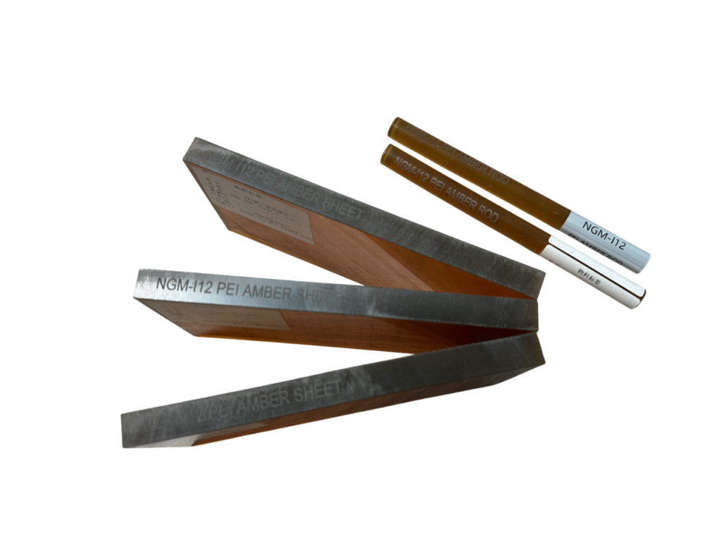
NAGOMER‘s ESD PEI (I6B grade) delivers these specifications consistently, with full lot traceability and certification documentation. Our material is processed under strict quality controls to ensure uniform ESD properties throughout the sheet or rod.
Applications in Semiconductor Test
ESD PEI finds applications throughout the semiconductor test flow:
Wafer probing – Probe card stiffeners and guides require the dimensional stability that PEI provides. Burn-in sockets – The heat resistance of PEI handles extended burn-in cycles at elevated temperatures. Handler contactors – The wear resistance and machinability of PEI enable precision contactor geometries. Test fixtures and nests – ESD protection prevents device damage during automated handling. Final test sockets – PEI‘s consistency ensures reliable electrical contact over thousands of test cycles.
With the transition to chiplets and advanced packaging, test complexity is increasing dramatically. ESD PEI will play an increasingly important role in enabling reliable, high-throughput semiconductor test operations.
Explore NAGOMER‘s complete ESD materials portfolio at nagomer.com. Request free samples and technical datasheets for ESD PEI today.