
News Centre
News Type
Send your inquiry
ESD PEEK in Semiconductor Equipment: Wafer Carriers, Test Sockets, and Process Components
Detailed guide to ESD-safe PEEK applications in semiconductor manufacturing equipment. Covers wafer carriers, test sockets, process components, and compliance with SEMI standards.
Introduction
Semiconductor manufacturing requires materials that combine: (1) ESD protection; (2) High temperature resistance; (3) Chemical resistance to process gases and liquids; (4) Low outgassing; (5) Dimensional stability. ESD PEEK delivers on all these requirements.
Why ESD PEEK for Semiconductor Equipment?
Standard PEEK is already widely used in semiconductor tools. Adding ESD protection (surface resistance 10^6-10^8 ohms) extends PEEK‘s utility to wafer handling and component applications where static discharge could damage devices.
Wafer Carriers and Cassettes
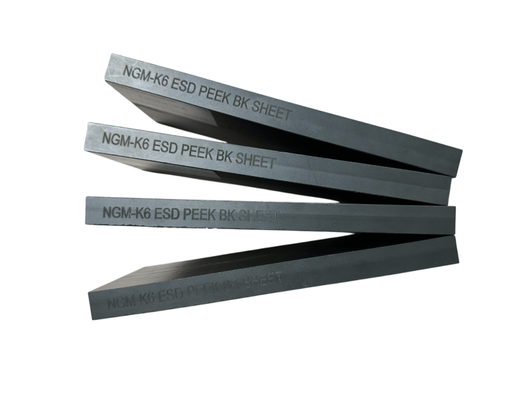
PEEK wafer carriers and cassettes offer: (1) Low particle generation; (2) Chemical resistance to cleaning solutions; (3) Dimensional stability across temperature cycles; (4) ESD protection for sensitive devices. NAGOMER ESD PEEK meets SEMI F57 standards for fluid compatibility.A
Test Sockets and Burn-in Sockets
Test sockets and burn-in sockets require materials that maintain dimensional stability at elevated temperatures (up to 150°C) while providing ESD protection. ESD PEEK sockets offer 2-3x longer life versus standard PEEK in high-cycle test applications.

Process Tool Components: Etch, CVD, and Wet Clean
In etch and CVD tools, PEEK components resist plasma exposure and aggressive process chemistries. ESD PEEK is used for: (1) Gas distribution components; (2) Wafer handling end-effectors; (3) Insulators and spacers; (4) Door seals and gaskets.
SEMI Standards Compliance for PEEK Components
SEMI standards relevant to PEEK components: (1) SEMI F57: Chemical compatibility of fluid system components; (2) SEMI F21: Particulate requirements for wafer containers; (3) SEMI E84: Electrical resistance measurement of static dissipative materials. NAGOMER ESD PEEK is tested per these standards.
Conclusion
As semiconductor device geometries shrink below 3nm, ESD sensitivity increases. ESD PEEK provides the protection needed while withstanding the harsh process environments in modern fabs. NAGOMER supplies ESD PEEK sheets, rods, and finished components to major semiconductor equipment manufacturers globally.
Contact NAGOMER today for a free sample and technical datasheet.