
News Centre
News Type
Send your inquiry
Engineering Plastics in Semiconductor Manufacturing Equipment 2026
Engineering Plastics in Semiconductor Manufacturing
Why Semiconductors Need Engineering Plastics
Semiconductor manufacturing requires materials that meet simultaneously demanding criteria:
1. Ultra-high purity — metallic contamination must be < 1 ppb
2. ESD protection — surface resistance 10^6–10^9 Ω/sq for device safety
3. Chemical resistance — withstand SC1, SC2, Piranha, HF, and other process chemicals
4. High temperature — RTP (rapid thermal processing) zones up to 300°C
5. Wear resistance — millions of wafer handling cycles
6. Dimensional stability — tolerances of ±0.025mm over large components
7. Low outgassing — compatible with ultra-high vacuum (UHV) environments
No single material meets all requirements — semiconductor fabs use a carefully selected palette of engineering plastics.
Material Selection by Process Area
Wafer Fabrication (Front-End)
Process Step | Key Materials | Critical Components |
Lithography | PEEK, PPS GF40 | Wafer stage pins, reticle chucks, alignment fixtures |
Etch (Dry) | PEEK, PPS | Chamber liners, electrode covers, gas distribution plates |
Etch (Wet) | PEEK, PTFE | Wet bench components, tank linings, spray nozzles |
CVD/PVD | PEEK, PEI | Chamber insulators, shield clips, substrate holders |
CMP | PEEK, ESD POM | Polishing ring guides, carrier head components, pad conditioners |
Ion Implant | PEEK, PPS | Beam line insulators, wafer handling end-effectors |
RTP/Anneal | PEEK | Wafer support rings, process tube components |
Wafer Test & Packaging (Back-End)
Process Step | Key Materials | Critical Components |
Wafer sort/test | ESD POM, PEEK | Test socket bodies, contactor housings, probe card components |
Dicing | PEEK, PTFE | Dicing tape frames, bonding fixtures |
Die attach | ESD POM, PPS | Pick-up tools, bond head tooling |
Wire bonding | ESD POM, PEI | Bonding fixture components, heat block insulators |
Moulding | PPS GF40 | Mould chase components, encapsulation tooling |
Trim/form | PEEK, ESD POM | Lead frame handling, tooling |
Final test | ESD POM, PEI | Test handlers, socket components |
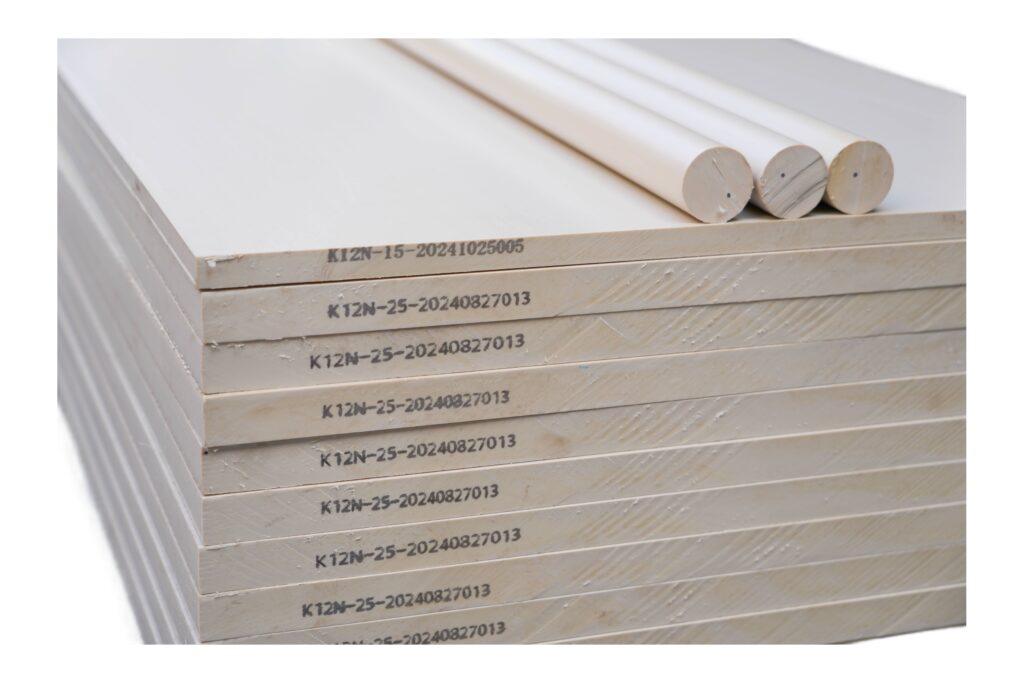
PEEK: The Semiconductor Workhorse
PEEK is the most critical engineering plastic in semiconductor manufacturing:
Key Semiconductor PEEK Applications
Wafer Carriers and Transport Cassettes
· Open cassettes for 200mm/300mm wafers
· Enclosed FOUP internal components
· Robot blade end-effectors
· Alignment notch tools
CMP (Chemical Mechanical Polishing)
· Polishing head ring guides (consumable)
· Retaining rings
· Pad conditioning disk holders
· Slurry distribution manifolds
Process Chamber Components
· CVD chamber liners (PEEK replaces quartz in some designs)
· PVD shield mounting clips
· Etch chamber electrode covers
· Vacuum chamber feedthrough insulators
Test & Inspection
· Probe card body components
· Test socket retainers (high-pin-count packages)
· Burn-in board insulators
· Handler interface components
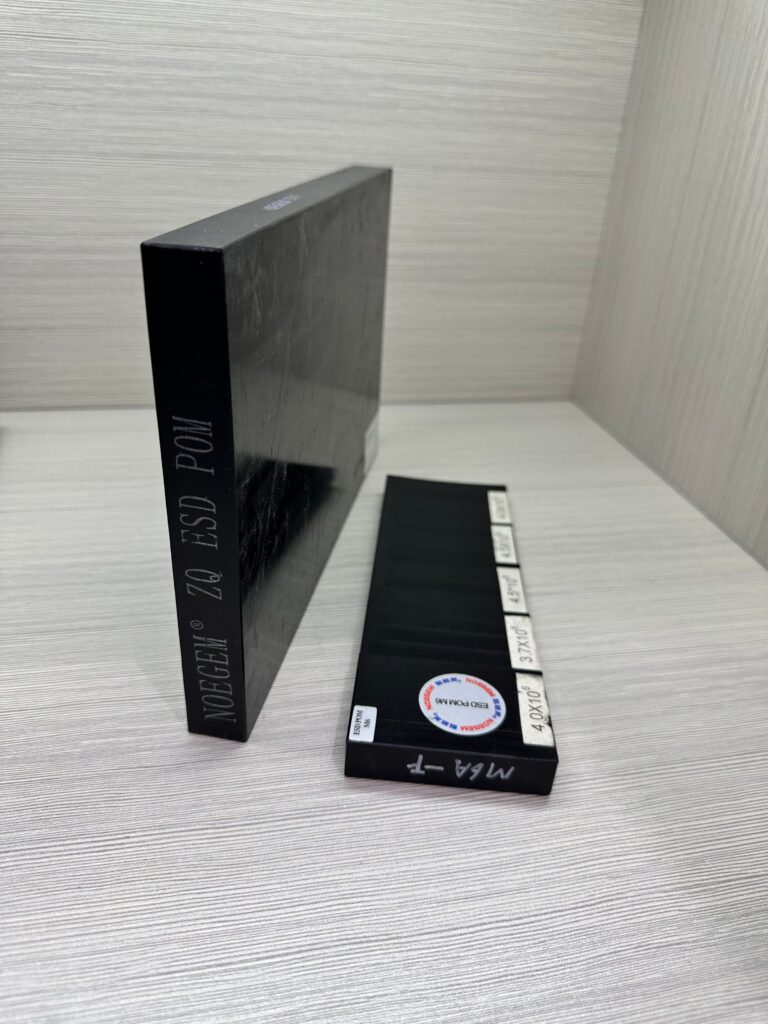
ESD POM: The Cost-Effective Alternative
For applications where temperature and chemical resistance are less critical, ESD POM provides ESD protection at 1/10th the cost of PEEK:
· Wafer handling trays and carriers (non-process areas)
· Test handler rails and escapements
· IC transport tubes and shipping materials
· Cleanroom furniture and workstations
· ESD-safe storage containers
For more on ESD POM in semiconductor, see our ESD POM Semiconductor Cleanroom guide. For material overview, read our Engineering Plastics Overview.
FAQ
Q1: Why is PEEK so widely used in semiconductor manufacturing?
PEEK combines ultra-high purity (metallic contamination < 1 ppb), high temperature resistance (250°C), excellent chemical resistance, outstanding wear resistance, and dimensional stability. No other material offers all these properties simultaneously, making PEEK indispensable in semiconductor wafer handling, CMP, and process chamber applications.
Q2: What is the difference between semiconductor-grade and industrial-grade PEEK?
Semiconductor-grade PEEK has lower metallic contamination levels (typically < 1 ppb vs < 10 ppb for industrial), tighter crystallinity control, and undergoes additional purity testing and certification. It costs 50–100% more than industrial grade PEEK.
Q3: Can ESD POM replace PEEK in semiconductor applications?
ESD POM can replace PEEK in non-process areas where temperature is below 90°C and chemical exposure is limited. Examples include wafer transport carriers outside the process area, test handler components, and cleanroom furniture. In process areas with high temperature or aggressive chemicals, PEEK remains essential.
Q4: What is the typical service life of PEEK semiconductor components?
PEEK semiconductor components typically last 6–24 months depending on the application. CMP ring guides are consumables replaced every 1–3 months. Wafer carrier components last 1–2 years. Chamber components can last 3–5 years with periodic maintenance.
Supplying engineering plastics for semiconductor manufacturing? Contact NAGOMER for ultra-pure PEEK and ESD materials, or explore our PEEK products and ESD POM.
NAGOMER — Professional Engineering Plastics Solutions
www.nagomer.com | info@nagomer.com