
News Centre
News Type
Send your inquiry
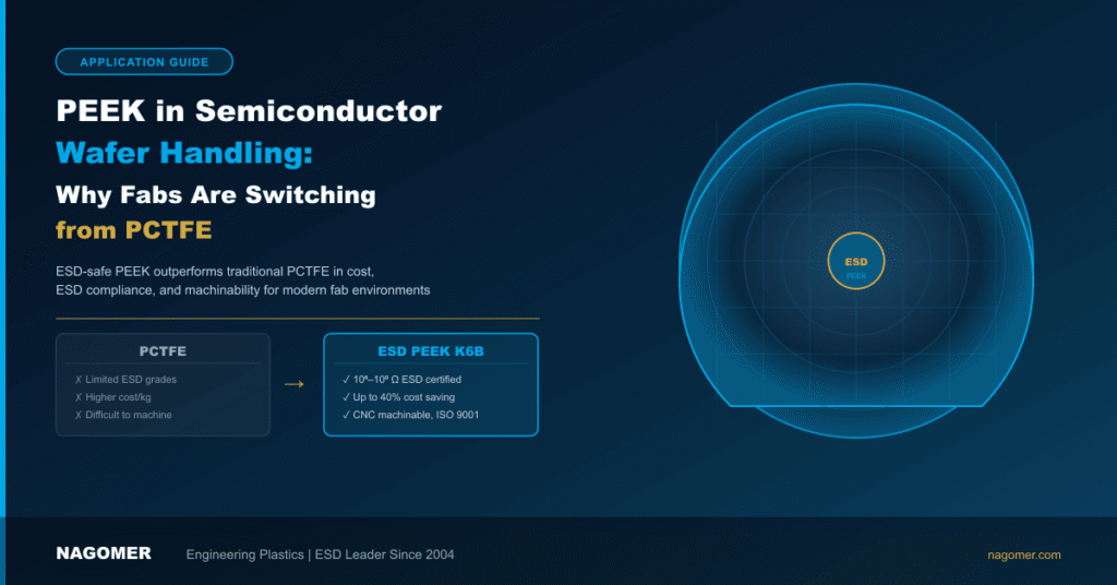
PEEK in Semiconductor Wafer Handling: Why Fabs Are Switching from PCTFE
For decades, PCTFE (Polychlorotrifluoroethylene) was the material of choice for wafer handling components in semiconductor fabrication — particularly for cassettes, carriers, and fixtures used in wet processing and chemical exposure environments. However, a significant shift is underway: leading semiconductor manufacturers are increasingly replacing PCTFE with ESD-grade PEEK, driven by compelling advantages in ESD compliance, cost, machinability, and long-term supply reliability.
This application guide examines why this transition is happening, where it is most applicable, and the key material properties that make ESD PEEK the preferred choice for modern 200mm and 300mm wafer handling environments.
What Is Wafer Handling in Semiconductor Manufacturing?
Wafer handling encompasses every step in which silicon wafers are moved, held, stored, or processed during semiconductor fabrication. The materials used for wafer handling components must satisfy an exceptionally demanding set of requirements:
• ESD control: No charge buildup that could discharge across sensitive IC structures on the wafer surface
• Ultra-high chemical purity: No extractables or leachables that could contaminate process chemicals or deposit on wafer surfaces
• Dimensional stability: Precise, repeatable dimensions to ensure proper wafer registration in automated handlers
• Temperature resistance: Some processes operate at elevated temperatures (up to 200°C+)
• Particle generation: Materials must not shed particles or fibers that could land on wafer surfaces
• Mechanical strength: Cassettes and carriers must withstand repeated load/unload cycles over millions of wafer moves

PCTFE: The Legacy Material and Its Limitations
PCTFE (also known by trade names including Kel-F, Neoflon, and Voltalef) has served the semiconductor industry well based on its exceptional chemical inertness and low moisture absorption. However, as fab requirements evolve, its limitations have become more pronounced:
PCTFE Limitation | Business Impact |
No native ESD grade available | Cannot meet IEC 61340-5 requirements; requires additional coatings or separate ESD elements |
High cost/kg ($80–$120 for standard grade) | Significantly higher material cost per wafer cassette vs. ESD PEEK |
Poor machinability | Higher CNC cycle time; short tool life; produces chips/burrs more than PEEK |
Limited supply chain (few producers) | Long lead times; price volatility; qualification risk for new suppliers |
Lower temperature capability vs PEEK | PCTFE max continuous service ~120°C vs. PEEK 260°C |
Particle shedding risk under stress | Polymer degradation under mechanical cycling can release particles into cleanroom |
Why ESD PEEK Is the Superior Alternative
ESD PEEK (NAGOMER grade K6B) directly addresses each of PCTFE’s limitations while maintaining comparable or superior performance in the properties that matter most for wafer handling:
1. Native ESD Compliance
ESD PEEK K6B is manufactured with consistent, stable surface resistivity of 10⁶–10⁸ Ω throughout the bulk material — not as a surface coating that can wear off. This means:
• Compliant with IEC 61340-5-1 and ANSI/ESD S4.1-2006 throughout the component lifetime
• No delamination or coating failure risk that could create uncontrolled static zones on the wafer handling surface
• Stable ESD performance maintained across the operating temperature range and after standard cleaning processes
2. Superior Chemical Resistance
PEEK offers outstanding resistance to the aggressive chemicals used in semiconductor wet processing:
• H₂SO₄/H₂O₂ (SPM/Piranha): Excellent resistance up to 150°C
• HF (Hydrofluoric Acid): Good resistance for short-contact applications
• NH₄OH/H₂O₂/H₂O (SC-1): Excellent resistance
• HCl/H₂O₂/H₂O (SC-2): Excellent resistance
• Acetone, IPA (isopropanol): Excellent resistance
• Strong bases (NaOH, KOH): Good resistance for most concentrations
| Chemical Resistance Note While PEEK offers excellent resistance to most semiconductor wet processing chemicals, concentrated sulfuric acid at very high temperatures and certain halogenated solvents at elevated temperatures can affect PEEK over prolonged exposure. Always validate with process-specific chemical exposure tests. NAGOMER’s technical team can assist with application review. |
3. Cost Advantage
At current market pricing:
• Standard PCTFE sheet: USD $80–$120/kg for standard grades
• ESD PEEK K6B (NAGOMER): USD $130–$155/kg — roughly comparable or slightly higher per kg
• However, PEEK’s superior machinability (faster CNC cycle times, longer tool life, better surface finish) typically delivers 20–35% lower finished-part cost even with comparable raw material cost
• For high-volume applications, NAGOMER’s direct manufacturing and 8,000+ ton/year capacity enables more competitive per-kg pricing than PCTFE specialty distributors
4. Machinability and Dimensional Control
PEEK is widely recognized as one of the most machinable engineering thermoplastics. Compared to PCTFE:
• Cutting speeds 30–50% faster with carbide tooling
• Superior surface finish (Ra < 0.4 μm achievable with standard practices)
• Excellent chip formation — no gummy or stringy chips that can contaminate machined surfaces
• Tight dimensional tolerances maintainable: ±0.05mm for critical features
• Lower residual stress after machining — better dimensional stability over time
Key Wafer Handling Applications for ESD PEEK
Wafer Cassettes and FOUP Inserts
Front Opening Unified Pod (FOUP) inserts and open cassettes are the highest-volume PEEK wafer handling component. ESD PEEK K6B ensures that wafers resting in the cassette slots are protected from ESD events while maintaining precise slot-to-slot pitch and smooth surface finish to prevent scratching.
End Effectors and Robot Paddles
Robotic arm end effectors that pick and place wafers require ESD-safe materials to prevent discharge during wafer contact. ESD PEEK K6B provides the stiffness, flatness, and ESD control required for 200mm and 300mm end effector applications.
Process Fixture Bodies and Clamps
Wet bench fixtures, chuck components, and process clamps made from ESD PEEK allow wafers to be held securely in chemical baths while maintaining ESD protection throughout the process.
Inspection and Metrology Fixtures
Wafer edge grip fixtures in metrology tools require materials with high dimensional stability and ESD control. ESD PEEK’s low thermal expansion and stable ESD properties make it ideal for critical measurement applications.
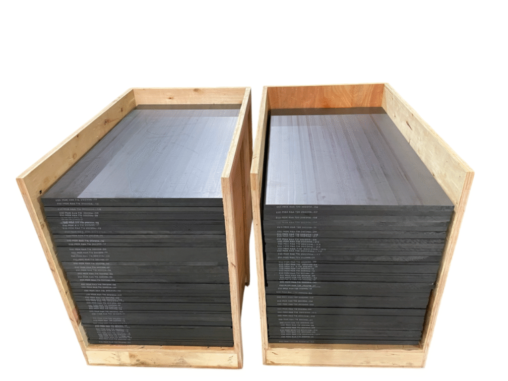
NAGOMER ESD PEEK: Grades and Specifications for Wafer Handling
Grade | Color | Resistivity | Key Features | Typical Wafer App |
Black | 10⁶–10⁸ Ω | Standard ESD PEEK, best machinability | Cassettes, paddles, fixtures | |
Black | 10²–10⁵ Ω | Conductive grade, rapid charge dissipation | Grounding fixtures, shields | |
Black | Insulative | Standard grade — NOT ESD-safe | Non-ESD structural parts only | |
Black | Insulative | Glass-filled, enhanced stiffness | High-stress structural parts |
Qualification Recommendations
For semiconductor fab teams evaluating ESD PEEK K6B as a replacement for PCTFE, NAGOMER recommends the following qualification steps:
- Request material certification package: ISO 9001 cert, surface resistivity test reports (per ANSI/ESD S4.1-2006), mechanical property data sheet
- Conduct chemical exposure testing: Immerse test coupons in your specific process chemicals for 24–72 hours and measure dimensional change, weight change, and surface resistivity before/after
- Machine a pilot fixture: Use NAGOMER-supplied sheet or rod to machine a pilot version of your cassette or fixture. Measure dimensional accuracy and surface finish
- Run a particle generation test: Measure particles shed by the machined part under simulated handling cycles — critical for cleanroom qualification
- Test ESD performance at operating conditions: Verify resistivity at actual operating temperature and humidity, not just room temperature
NAGOMER Application Support NAGOMER’s technical team works directly with semiconductor component manufacturers and end-user fabs to qualify ESD PEEK for wafer handling applications. We provide sample material for qualification testing, technical data packages, and application-specific engineering support. Contact us to start the qualification process. |
Conclusion
The transition from PCTFE to ESD PEEK in semiconductor wafer handling is not a trend — it is an industry shift driven by compelling technical and economic advantages. ESD PEEK K6B offers native ESD compliance, superior machinability, competitive total cost, and excellent chemical resistance that matches or exceeds PCTFE performance in the vast majority of wafer handling applications.
For fabs looking to improve ESD control, reduce per-fixture cost, and secure a more reliable supply chain for wafer handling plastics, ESD PEEK represents the most logical material evolution — and NAGOMER is positioned to support the transition at scale.