
News Centre
News Type
Send your inquiry
ESD POM in Semiconductor Cleanroom: Preventing Electrostatic Discharge Damage
The ESD Threat in Semiconductor Fabs
How Static Charges Build Up
In a cleanroom environment, static charges accumulate through:
· Triboelectric charging — wafer contact/separation with transport fixtures and carriers
· Air friction — high-velocity airflow in laminar flow hoods (0.3–0.5 m/s)
· Insulator induction — charged insulators (standard plastics, rubber, glass) inducing charge on nearby conductors
· Process-induced charging — plasma etching, ion implantation, and CMP processes
At advanced nodes (7nm and below), device sensitivity thresholds can be as low as 20V for HBM (Human Body Model) and 5V for CDM (Charged Device Model).
Cost of ESD Damage
Damage Type | Cost Impact | Detection |
Catastrophic failure | Device destroyed | Immediate — caught at test |
Latent failure | Reduced lifespan | Difficult — field return |
Parametric drift | Performance degradation | Possible at ATE |
Yield loss | Scrap wafer/batch | Caught at wafer sort |
Industry estimates suggest ESD-related losses of 4–8% of annual revenue in semiconductor manufacturing — representing billions of dollars globally.
ESD POM: The Cleanroom Solution
Why ESD POM Instead of Other ESD Materials?
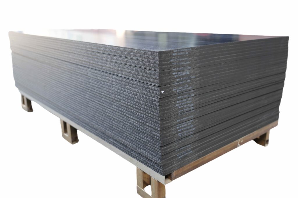
ESD POM is the preferred material for semiconductor cleanroom components because:
1. Cost-effective — 3–5× cheaper than ESD PEEK for non-critical components
2. Machinability — excellent CNC machinability for complex geometries
3. Wear resistance — suitable for repeated-use wafer handling components
4. Low particle generation — hard, crystalline surface generates fewer particles than softer materials
5. Chemical stability — resists cleaning chemicals (IPA, SC1, SC2, Piranha)
6. Dimensional stability — low moisture absorption maintains tolerances
Cleanroom Compatibility of ESD POM
|
Property |
Requirement |
ESD POM Performance |
|
Surface resistance |
10^6–10^9 Ω/sq |
✓ Meets |
|
Particle generation (ISO 5) |
< 1 particle/min |
✓ Meets |
|
Outgassing (TML) |
< 1.0% |
✓ < 0.5% |
|
Outgassing (CVCM) |
< 0.1% |
✓ < 0.05% |
|
Chemical resistance |
IPA, acetone, mild acids |
✓ Resistant |
|
Cleanroom class |
ISO 4 or better |
✓ Compatible |
Key Semiconductor Applications of ESD POM
Wafer Handling & Transport
· Open cassettes — 150mm, 200mm, 300mm wafer carriers with ESD-safe pockets
· FOUP (Front Opening Unified Pod) components — internal support structures and wafer separators
· Transfer modules — robotic arm end-effectors and gripper inserts
· Alignment fixtures — notch alignment and orientation tools
Process Equipment Components
· CMP ring guides — chemical mechanical polishing consumables
· Etch chamber liners — plasma etch process kit components
· Lithography stage pins — wafer stage locating pins
· Sputter shield clips — PVD chamber consumables
Test & Assembly
· Test socket bodies — burn-in and test interface components
· IC tray pockets — molded tray for finished device transport
· Lead frame carriers — die attach and wire bond stage tooling
· Marking fixtures — laser marking stage tooling
Cleanroom Infrastructure
· Workstation tops — ESD-safe work surfaces
· Shelving and storage bins — wafer bank storage
· Cart wheels and casters — ESD-safe mobility
· Chair components — cleanroom-compatible seating
For more on ESD POM properties, see our ESD POM vs Standard POM guide. For ESD material selection, read our ESD Plastic Materials guide.
FAQ
Q1: What cleanroom class is ESD POM compatible with?
Properly processed and cleaned ESD POM components are compatible with ISO Class 4 (Class 10) cleanrooms. For ultra-clean ISO Class 3 (Class 1) environments, additional cleaning protocols and low-outgassing verification may be required.
Q2: How does ESD POM prevent wafer damage?
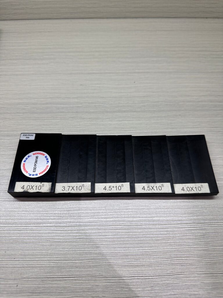
ESD POM has a surface resistance of 10^6–10^9 ohms per square, which allows static charges to dissipate safely through the material. This prevents charge accumulation on wafer handling components that could discharge into the wafer, causing device damage or destruction.
Q3: Can ESD POM be used in FOUP (wafer pod) components?
Yes, ESD POM is commonly used for internal FOUP components such as wafer separators, support rails, and alignment features. However, the FOUP body itself typically uses more chemically resistant materials like PEEK or PPS for compatibility with harsh fab environments.
Q4: How often should ESD POM cleanroom components be replaced?
Replacement frequency depends on usage conditions. Typically, ESD POM wafer handling components are replaced based on particle count, surface resistance verification, or visual wear inspection. Most components have a service life of 6–24 months in normal cleanroom use.
Protect your semiconductor wafers with ESD POM from NAGOMER. Contact us for cleanroom-grade ESD materials, or explore our ESD POM products and POM rod catalogue.
NAGOMER — Professional Engineering Plastics Solutions
www.nagomer.com | info@nagomer.com