
News Centre
News Type
Send your inquiry
ESD POM for Semiconductor IC Trays and Packaging: NAGOMER NFP Series Innovation
Semiconductor Packaging: The Final ESD Frontier
After wafers are fabricated, tested, diced, and packaged into individual ICs, the finished components enter the semiconductor packaging and logistics chain. At this stage, the devices are at their most vulnerable: they have value (often $10-100+ per component), they are being handled at high speed in automated equipment, and ESD protection is the last line of defense before shipment to customers.
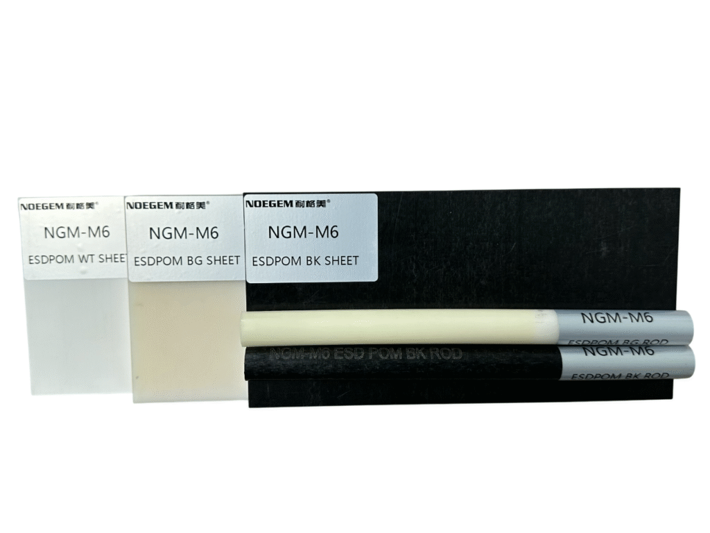
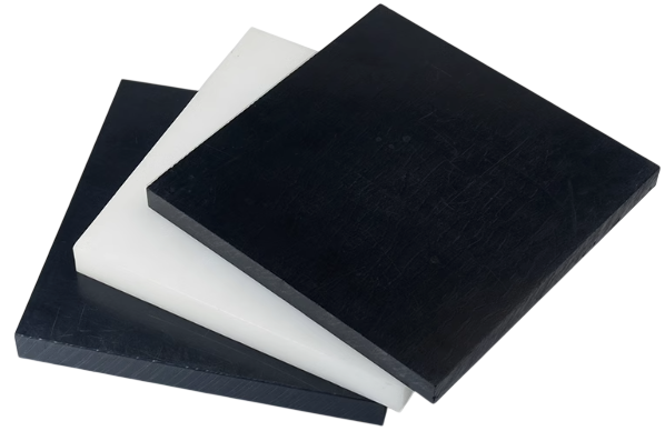
ESD POM (acetal) has become one of the most important materials for semiconductor component handling and packaging. Its combination of static dissipation, mechanical durability, clean operation, and cost-effectiveness makes it the material of choice for IC trays, carrier tapes, and handling fixtures at the packaging stage.
NAGOMER‘s NFP (Non-Flaking Powder) series represents a breakthrough in ESD POM technology, addressing the critical issue of carbon particle shedding that has historically limited the use of conductive plastics in clean packaging applications.
The Problem with Traditional Conductive POM
Traditional ESD and conductive POM achieves its electrical properties through the addition of conductive carbon black. While effective for static dissipation, this approach has a well-known limitation:
Carbon particle shedding: The carbon black particles at the surface of the material can become dislodged through friction, vibration, or contact. These microscopic carbon particles can contaminate sensitive electronic components, causing short circuits or reliability issues.
Powder contamination: Over time, carbon-filled POM components can develop a visible layer of black powder on their surface. In semiconductor packaging environments, this contamination is unacceptable.
Inconsistent resistivity: Carbon black dispersion can vary, leading to hot spots (areas of higher conductivity) and dead zones (areas of insufficient conductivity).
These limitations have historically forced semiconductor manufacturers to either accept the contamination risk, use more expensive materials (like ESD PEI or PEEK), or implement additional cleaning and inspection steps.
NAGOMER NFP Series: The Solution
NAGOMER‘s NFP (Non-Flaking Powder) series of ESD POM represents a significant technological advancement:
Zero powder technology: Through proprietary formulation and processing, NFP grades achieve consistent static dissipation (10^6-10^8 ohms per square) without the carbon particle shedding that plagues traditional conductive POM. Surface powder testing per industry standards confirms zero detectable particle generation.
Consistent resistivity: Advanced compounding technology ensures uniform dispersion of the conductive phase throughout the material, eliminating hot spots and dead zones. Resistivity variation across a sheet is less than half an order of magnitude.
Excellent mechanical properties: NFP grades maintain the mechanical properties of standard POM-C, including tensile strength of 65+ MPa, flexural modulus of 2,600+ MPa, and excellent machinability.
Cost advantage: NFP ESD POM costs approximately 40-60% less than ESD PEI and 60-80% less than ESD PEEK, providing significant cost savings for high-volume packaging applications.
NFP series is currently the only ESD POM worldwide with verified zero-powder performance, making NAGOMER the leader in this technology.
Applications in Semiconductor Packaging
ESD POM, particularly NFP grades, is used throughout the semiconductor packaging process:
IC trays (JEDEC trays): These trays hold finished ICs during testing, baking, marking, and shipping. ESD POM provides the static protection, dimensional stability, and clean operation these applications demand.
Carrier tape pockets: Surface mount components are packaged in carrier tape with formed pockets. ESD POM (as the tape material or insert) provides static protection during automated pick-and-place assembly.
Component handling fixtures: Test sockets, pick-and-place nozzles, and assembly fixtures in semiconductor packaging lines benefit from ESD POM‘s combination of machinability, wear resistance, and static dissipation.
Shipping and storage: Trays, tubes, and magazines for component shipping and warehousing use ESD POM for long-term ESD protection.
NAGOMER‘s NFP series is particularly valued in applications where carbon particle contamination has historically been a concern.
Material Comparison for Packaging Applications
For semiconductor packaging applications, the key material options:
ESD POM NFP Series (NAGOMER): Best cost-performance ratio for high-volume packaging. Zero powder for clean applications. 10^6-10^8 ohms/sq. Recommended for most IC tray and carrier tape applications.
ESD PEI (NAGOMER I6B): Higher temperature resistance (200C+) for applications involving elevated temperatures. Better dimensional stability. Lower particle emission. 30-50% higher cost than ESD POM.
ESD PEEK (NAGOMER K6B): Ultimate performance for the most demanding applications. Highest temperature resistance (260C). Lowest outgassing. Best mechanical properties. 3-5x cost of ESD POM. Reserved for critical applications.
The majority of semiconductor packaging applications are well served by NFP ESD POM, which provides the essential ESD protection and clean operation at an economical cost.
Discover NAGOMER‘s NFP series – the world’s only zero-powder ESD POM. Visit nagomer.com for samples and technical documentation.