
News Centre
News Type
Send your inquiry
ESD PPS for Wafer Handling: Precision, Purity, and Static Control in Semiconductor Manufacturing
Semiconductor Manufacturing: Where Precision Meets Purity
Semiconductor wafer fabrication is perhaps the most demanding manufacturing environment on Earth. A single speck of dust can render a multi-million-dollar wafer useless. A static discharge can destroy weeks of fabrication work in microseconds. Chemical purity requirements are measured in parts per billion.
At advanced process nodes (3nm, 2nm), these requirements become exponentially more stringent. The materials that handle wafers through hundreds of process steps must maintain their properties through aggressive chemical exposure, temperature extremes, and mechanical stress, all while never introducing contamination or generating static charge.
ESD (electrostatic dissipative) PPS has emerged as a critical material for semiconductor wafer handling applications. Its unique combination of properties addresses the semiconductor industry’s most demanding requirements.
Why ESD PPS for Wafer Handling
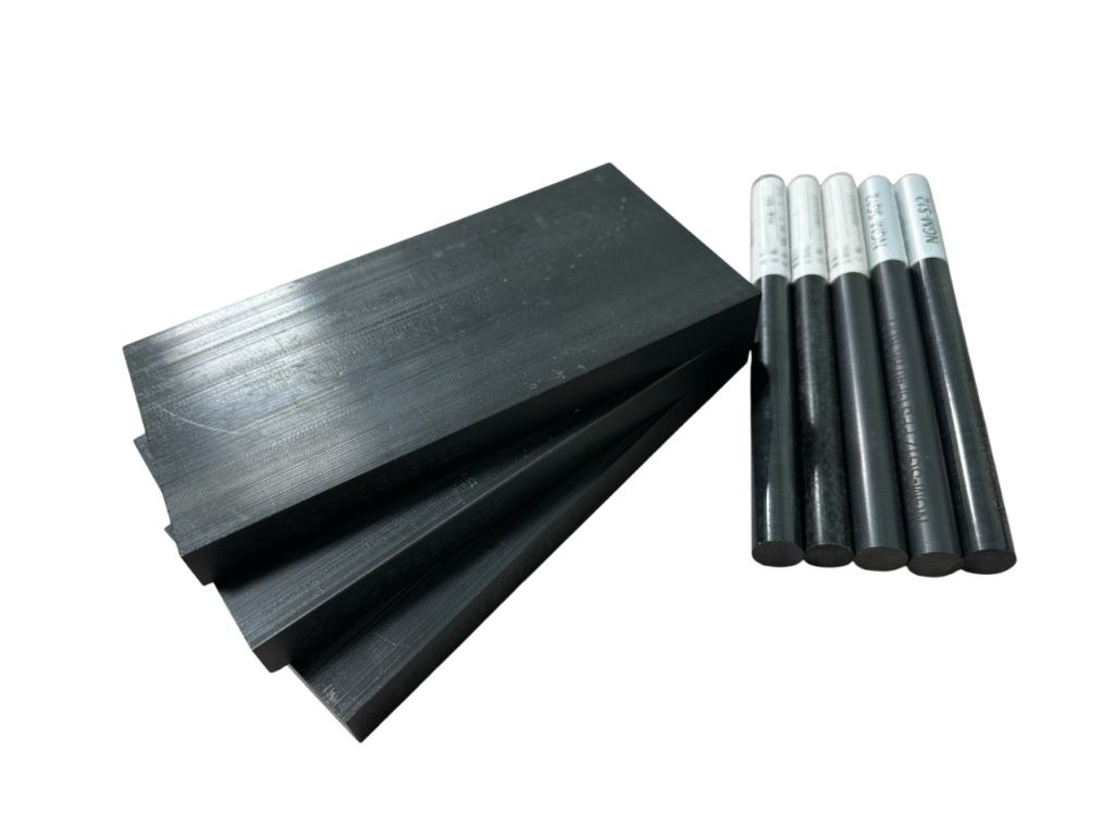
ESD PPS offers a distinctive combination of properties ideal for wafer handling:
Controlled static dissipation: Surface resistivity 10^6-10^8 ohms/square provides predictable, consistent static dissipation without the variability of carbon-filled materials. This is critical for protecting devices with ever-decreasing gate oxide thicknesses.
Exceptional chemical resistance: PPS is virtually immune to the aggressive chemicals used in semiconductor processing, including HF, HCl, H2SO4, NH4OH, and H2O2 in various combinations. Unlike many materials, PPS does not degrade, swell, or leach contaminants even after thousands of chemical exposure cycles.
Ultra-low particle generation: Properly processed ESD PPS produces extremely low particle counts, maintaining cleanroom classification even in ISO Class 3 and better environments.
High-temperature capability: With HDT of 260C, ESD PPS handles process temperatures that would degrade or deform lower-performance materials.
Applications in the Semiconductor Fab
ESD PPS is used throughout the semiconductor manufacturing process:
Wafer carriers and cassettes: These transport wafers between process tools, through wet benches, and into furnaces. ESD PPS carriers protect wafers from ESD damage while resisting chemical attack from residual process chemicals.
Process trays for wet processing: During cleaning, etching, and stripping operations, wafers sit in process trays immersed in aggressive chemical baths. ESD PPS maintains dimensional stability and chemical resistance through thousands of cycles.
FOUP (Front Opening Unified Pod) components: The automated material handling system that moves wafers between tools in 300mm fabs requires materials with precise dimensional control and particle-free operation.
End effectors for wafer handling robots: The wafer handling fingers that pick and place wafers must be static-dissipative to prevent ESD events during wafer transfer, while maintaining the precision needed for sub-millimeter positioning.
ESD PPS vs ESD PEEK vs ESD PEI
When selecting materials for semiconductor wafer handling, engineers typically evaluate three high-performance ESD materials:
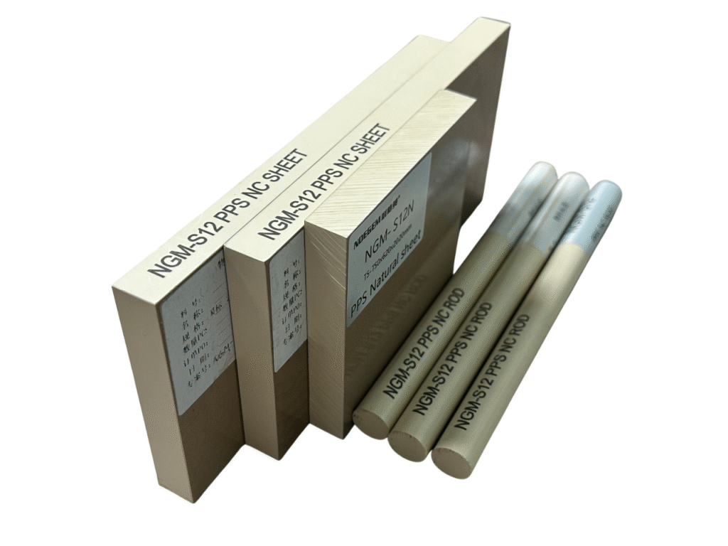
ESD PPS (NAGOMER S6B): Best overall chemical resistance, highest temperature capability, lowest moisture absorption. Best choice for wet process applications and high-temperature processes. Cost-effective for high-volume applications.
ESD PEEK (NAGOMER K6B): Highest mechanical strength, best wear resistance, lowest outgassing. Best choice for critical applications requiring the ultimate in purity and performance. Higher cost but justified for the most demanding applications.
ESD PEI (NAGOMER I6B): Best machinability, good balance of properties, moderate cost. Good choice for less aggressive chemical environments and applications requiring complex machined geometries.
For most wafer handling applications, ESD PPS provides the optimal balance of performance and cost. It matches or exceeds PEEK in chemical resistance while offering significant cost advantages at production volumes.
Quality and Certification for Semiconductor Supply
Semiconductor industry suppliers must meet rigorous quality requirements:
Material certification: Every lot must be accompanied by certificate of analysis including resistivity measurement, mechanical properties, and chemical composition. NAGOMER provides full lot traceability.
Surface resistivity testing: Per ANSI/ESD S4.1 (DIN IEC 60093), resistivity must be verified on every production lot and documented.
Cleanroom packaging: Materials for semiconductor use must be packaged in cleanroom-compatible packaging and shipped under controlled conditions.
Change notification: Semiconductor customers require advance notification of any material or process changes, typically 6-12 months, to allow for requalification.
NAGOMER‘s quality management system (ISO 9001:2015 certified) meets these requirements, and we work closely with semiconductor customers to ensure consistent, reliable supply.
Contact NAGOMER for ESD PPS samples and semiconductor-grade material certification. Visit nagomer.com for complete technical documentation.